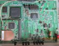
Linksys WRV54G v1
Linksys WRV54G v1
Manuf (OEM/ODM): Gemtek WX5715 V0.1
FCC approval date: 01 August 2003
(Est.) release date: March 2004
UPC: 745883556687 (UPC DB, On eBay)
Country of manuf.: Taiwan

Type: wireless router
FCC ID: Q87-WRV54G
IC ID: 3839A-WRV54G
Power: 5 VDC, 2.5 A
Connector type: barrel
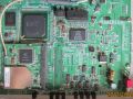
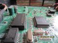
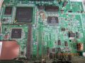
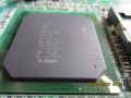
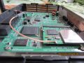
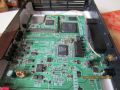
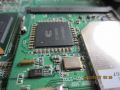
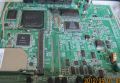
CPU1: Intel XScale IXP425 (266 MHz)
FLA1: 8 MiB8,388,608 B <br />65,536 Kib <br />8,192 KiB <br />64 Mib <br />0.00781 GiB <br /> (Intel E28F640J3A-120)
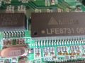
RAM1: 32 MiB33,554,432 B <br />262,144 Kib <br />32,768 KiB <br />256 Mib <br />0.0313 GiB <br /> (Dynachips D98SD12816AH-6 × 2)
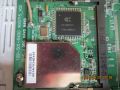
Expansion IFs: Mini PCI
Mini PCI slots: 1
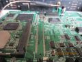
JTAG: yes, 20-pin header, J2
Serial: yes, 9-pin header
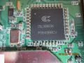
WI1 module: unknown
WI1 module IF: Mini PCI
WI1 chip1: Intersil ISL3880
WI1 chip2: Intersil ISL3686A
WI1 802dot11 protocols: bg
WI1 antenna connector: U.FL, RP-SMA
ETH chip1: Intel XScale IXP425
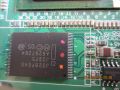
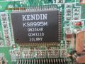
Switch: Kendin KS8995M
LAN speed: 100M
LAN ports: 4
WAN speed: 100M
WAN ports: 1
bg
802dot11 OUI: 00:12:17 (16 E, 32 W), 00:1A:70 (9 E, 15 W)
Ethernet OUI: 00:12:17 (16 E, 32 W), 00:1A:70 (9 E, 15 W)
| CPU1 brand | WI1 chip1 brand | WI1 chip2 brand | |
|---|---|---|---|
| Linksys WRV54G v1 | Intel XScale | Intersil | Intersil |
| Linksys WRV54G v2 | Intel XScale | Ralink | Ralink |
For a list of all currently documented Intel XScale SoC's with specifications, see Intel XScale.
For a list of all currently documented Intersil chipsets with specifications, see Intersil.
Additional FCC IDs of Q87-HGA7S-3 (Linksys HGA7S, high gain antenna)
- and Q87-HGA5S-3 (Linksys HGA5S, high gain antenna)
WRV54G v1 serial numbers appear to start with MEX0.
- The default SSID may be linksys-g.
OEM: Gemtek WX5715 (WX5715_V01)
- The CPU is part FWIXP425AB.
- Wi-Fi Certified : W001244 (as of 04/29/2004)
Links
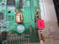
Serial
- Serial Port Pinout
On the WRV-54G board, the 9 pins look like:
              -----
(ttyS1 TX) 1 | 0 o | 2  +3.3V
           3 | o o | 4  +3.3V
           5 | o o | 6  GND
(ttyS1 RX) 7 | o o | 8  GND
           9 | o   |
              -----
(I've renumbered the pins to the standard pin convention for these connectors)
JTAG
J2 is definitely JTAG. It is using the 20-pin standard ARM JTAG pin layout.
- Pin 1 on this header is on the edge of the board, closest to the LED.
Pinout: (from Intel)
                c[] LED5
       +3.3V -- 1 o o 2 -- NC
       nTRST -- 3 o o 4 -- GND
         TDI -- 5 o o 6 -- GND
         TMS -- 7 o o 8 -- GND
         TCK -- 9 o o 10 - GND
         GND - 11 o o 12 - GND
         TDO - 13 o o 14 - GND
      nRESET - 15 o o 16 - GND
          NC - 17 o o 18 - GND
          NC - 19 o o 20 - GND
Images
- unsourced images